www.vishay.com
V20WM100C-M3
Vishay General Semiconductor
Dual Trench MOS Barrier Schottky Rectifier
Ultra Low VF = 0.5...
www.vishay.com
V20WM100C-M3
Vishay General Semiconductor
Dual Trench MOS Barrier Schottky Rectifier
Ultra Low VF = 0.53 V at IF = 5 A
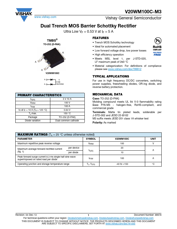
TMBS®
TO-252 (D-PAK)
K
A
A V20WM100C
AK A HEATSINK
FEATURES Trench MOS Schottky technology Ideal for automated placement Low forward
voltage drop, low power losses High efficiency operation Meets MSL level 1, per J-STD-020,
LF maximum peak of 260 °C Material categorization: For definitions of compliance
please see www.vishay.com/doc?99912
TYPICAL APPLICATIONS For use in high frequency DC/DC converters, switching power supplies, freewheeling diodes, OR-ing diode, and reverse battery protection.
PRIMARY CHARACTERISTICS
IF(AV) VRRM IFSM VF at IF = 10 A (TA = 125 °C) TJ max. Package
2 x 10 A 100 V 100 A 0.64 V 150 °C
TO-252 (D-PAK)
Diode variation
Dual common cathode
MECHANICAL DATA
Case: TO-252 (D-PAK) Molding compound meets UL 94 V-0 flammability rating Base P/N-M3 - halogen-free, RoHS-compliant, and commercial grade
Terminals: Matte tin plated leads, solderable per J-STD-002 and JESD 22-B102 M3 suffix meets JESD 201 class 1A whisker test
Polarity: As marked
MAXIMUM RATINGS (TA = 25 °C unless otherwise noted)
PARAMETER
SYMBOL
Maximum repetitive peak reverse
voltage
Maximum average forward rectified current (fig. 1)
per device per diode
VRRM IF(AV)
Peak forward surge current 8.3 ms single half sine-wave superimposed on rated load per diode
IFSM
Operating junction and storage temperature range
TJ, TSTG
V20WM100C...