New Product
V40100G, VF40100G, VB40100G & VI40100G
www.DataSheet4U.com Vishay General Semiconductor
Dual High-Voltage ...
New Product
V40100G, VF40100G, VB40100G & VI40100G
www.DataSheet4U.com Vishay General Semiconductor
Dual High-
Voltage Trench MOS Barrier Schottky Rectifier
Ultra Low VF = 0.42 V at IF = 5 A
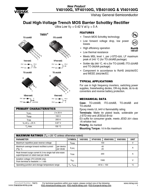
TMBS ®
TO-220AB ITO-220AB
FEATURES Trench MOS Schottky technology Low forward
voltage drop, low power losses High efficiency operation Low thermal resistance
2 V40100G
PIN 1 PIN 3 PIN 2 CASE
3 1 VF40100G
PIN 1 PIN 3 PIN 2
2
3
1
Meets MSL level 1, per J-STD-020, LF maximum peak of 245 °C (for TO-263AB package) Solder dip 260 °C, 40 s (for TO-220AB, ITO-220AB and TO-262AA package) Component in accordance to RoHS 2002/95/EC and WEEE 2002/96/EC TYPICAL APPLICATIONS
TO-263AB K K
TO-262AA
2 1 1 VB40100G
PIN 1 PIN 2 K HEATSINK
2
3
For use in high frequency inverters, switching power supplies, freewheeling diodes, OR-ing diode, dc-to-dc converters and reverse battery protection. MECHANICAL DATA Case: TO-220AB, ITO-220AB, TO-263AB and TO-262AA Epoxy meets UL 94V-0 flammability rating Terminals: Matte tin plated leads, solderable per J-STD-002 and JESD22-B102 E3 suffix for consumer grade, meets JESD 201 class 1A whisker test Polarity: As marked Mounting Torque: 10 in-lbs maximum
VI40100G
PIN 1 PIN 3 PIN 2 K
PRIMARY CHARACTERISTICS
IF(AV) VRRM IFSM VF at IF = 20 A TJ max. 2 x 20 A 100 V 200 A 0.67 V 150 °C
MAXIMUM RATINGS (TA = 25 °C unless otherwise noted)
PARAMETER Maximum repetitive peak reverse
voltage Maximum average forward rectified current (Fig. 1) per device p...