www.DataSheet.co.kr
New Product
VT4060C, VIT4060C
Vishay General Semiconductor
Dual Trench MOS Barrier Schottky Recti...
www.DataSheet.co.kr
New Product
VT4060C, VIT4060C
Vishay General Semiconductor
Dual Trench MOS Barrier Schottky Rectifier
Ultra Low VF = 0.32 V at IF = 5.0 A
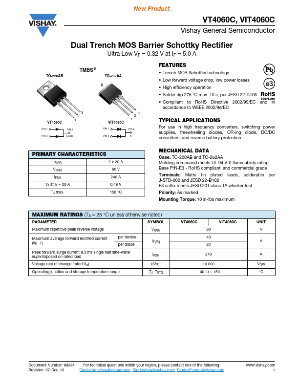
TMBS ®
TO-220AB K TO-262AA
FEATURES
Trench MOS Schottky technology Low forward
voltage drop, low power losses High efficiency operation Solder dip 275 °C max. 10 s, per JESD 22-B106 Compliant to RoHS Directive 2002/95/EC and in accordance to WEEE 2002/96/EC
2 VT4060C
PIN 1 PIN 3 PIN 2 CASE
3 1 VIT4060C
PIN 1 PIN 3
2
3
1
TYPICAL APPLICATIONS
For use in high frequency converters, switching power supplies, freewheeling diodes, OR-ing diode, DC/DC converters, and reverse battery protection.
PIN 2 K
PRIMARY CHARACTERISTICS
IF(AV) VRRM IFSM VF at IF = 20 A TJ max. 2 x 20 A 60 V 240 A 0.48 V 150 °C
MECHANICAL DATA
Case: TO-220AB and TO-262AA Molding compound meets UL 94 V-0 flammability rating Base P/N-E3 - RoHS compliant, and commercial grade Terminals: Matte tin plated leads, solderable J-STD-002 and JESD 22-B102 E3 suffix meets JESD 201 class 1A whisker test Polarity: As marked Mounting Torque: 10 in-lbs maximum per
MAXIMUM RATINGS (TA = 25 °C unless otherwise noted)
PARAMETER Maximum repetitive peak reverse
voltage Maximum average forward rectified current (fig. 1) per device per diode IF(AV) IFSM dV/dt TJ, TSTG SYMBOL VRRM VT4060C 60 40 A 20 240 10 000 - 40 to + 150 A V/μs °C VIT4060C UNIT V
Peak forward surge current 8.3 ms single half sine-wave superimposed on rated load
Voltage rate of change (r...