Spread Spectrum FTG for VIA K7 Chipset
W210
Spread Spectrum FTG for VIA K7 Chipset
Features
• Maximized EMI Suppression using Cypress’s Spread Spectrum techno...
Description
W210
Spread Spectrum FTG for VIA K7 Chipset
Features
Maximized EMI Suppression using Cypress’s Spread Spectrum technology Single-chip system frequency synthesizer for VIA K7 chipset One pair of differential CPU outputs for K7 Processor One open-drain CPU output for VIA K7 chipset Six copies of PCI output One 48-MHz output for USB One 24-MHz or 48-MHz output for SIO Two buffered reference outputs Thirteen SDRAM outputs provide support for 3 DIMMs Supports frequencies up to 200 MHz I2C™ interface for programming Power management control inputs Available in 48-pin SSOP Table 1. Mode Input Table Mode 0 1 Pin 2 CPU_STOP# REF0
Key Specifications
CPU to CPU Output Skew: ......................................... 175 ps PCI to PCI Output Skew: ............................................ 500 ps VDDQ3: .................................................................... 3.3V±5%
Table 2. Pin Selectable Frequency Input Address CPU FS3 FS2 FS1 FS0 (MHz) 1 1 1 1 133.3 1 1 1 0 75 1 1 0 1 100.2 1 1 0 0 66.8 1 0 1 1 79 1 0 1 0 110 1 0 0 1 115 1 0 0 0 120 0 1 1 1 133.3 0 1 1 0 83.3 0 1 0 1 100.2 0 1 0 0 66.8 0 0 1 1 124 0 0 1 0 129 0 0 0 1 138 0 0 0 0 143
PCI0:5 (MHz) 33.3 37.5 33.3 33.4 39.5 36.7 38.3 30 33.3 27.7 33.3 33.4 31.0 32.3 34.5 35.8
Spread Spectrum ±0.5% ±0.5% ±0.5% ±0.5% OFF OFF OFF OFF OFF OFF OFF OFF OFF OFF OFF OFF
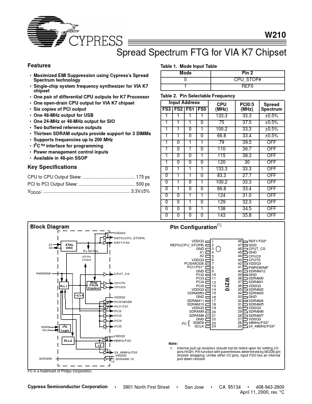
Block Diagram
VDDQ3 REF0/(CPU_STOP#) X1 X2 XTAL OSC
PLL Ref Freq
Pin Configuration
REF1/FS0
[1]
I/O Pin Control
PWRDWN#
CPUT_CS ...
Similar Datasheet