Features
� 2A,650V(Type),RDS(on)(Max 5Ω)@VGS=10V � Ultra-low Gate Charge(Typical 9.0nC) � Fast Switching Capability � 10...
Features
� 2A,650V(Type),RDS(on)(Max 5Ω)@VGS=10V � Ultra-low Gate Charge(Typical 9.0nC) � Fast Switching Capability � 100%Avalanche Tested � Isolation
Voltage(VISO=4000V AC) � Maximum Junction Temperature Range(150℃)
WFF2N65B
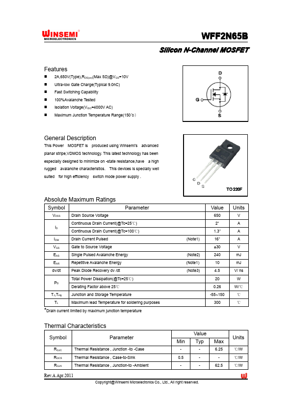
Silicon N-Channel
MOSFET
General Description
This Power
MOSFET is produced using Winsemi's advanced planar stripe,VDMOS technology. This latest technology has been especially designed to minimize on -state resistance,have a high rugged avalanche characteristics. This devices is specially well suited for high efficiency switch mode power supply .
Absolute Maximum Ratings
Symbol
Parameter
VDSS ID
Drain Source
Voltage Continuous Drain Current(@Tc=25℃) Continuous Drain Current(@Tc=100℃)
IDM Drain Current Pulsed
VGS Gate to Source
Voltage
EAS Single Pulsed Avalanche Energy
EAR Repetitive Avalanche Energy
dv/dt
Peak Diode Recovery dv /dt
Total Power Dissipation(@Tc=25℃) PD
Derating Factor above 25℃
TJ,Tstg
Junction and Storage Temperature
TL Maximum lead Temperature for soldering purposes
*Drain current limited by maximum junction temperature
(Note1)
(Note2) (Note1) (Note3)
Value
650 2* 1.3* 16* ±30 240 10 4.5 20 0.26 -55~150 300
Units
V A A A V mJ mJ V/ ns W W/℃ ℃ ℃
Thermal Characteristics
Symbol
Parameter
RQJC RQCS RQJA
Thermal Resistance , Junction -to -Case Thermal Resistance , Case-to-Sink Thermal Resistance , Junction-to -Ambient
Value Min Typ
-0.5 -
--
Rev.A Apr.2011
Copyright@Winsemi Microelectronics Co., Ltd., All right res...