36.0-43.0 GHz GaAs MMIC Buffer Amplifier
April 2005 - Rev 01-Apr-05
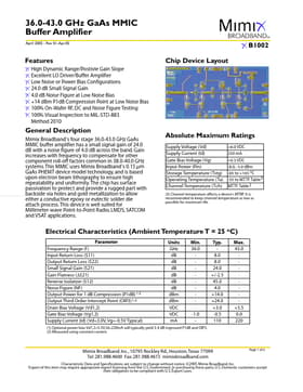
B1002 Chip Device Layout
Features
High Dynamic Ran...
36.0-43.0 GHz GaAs MMIC Buffer Amplifier
April 2005 - Rev 01-Apr-05
B1002 Chip Device Layout
Features
High Dynamic Range/Postivie Gain Slope Excellent LO Driver/Buffer Amplifier Low Noise or Power Bias Configurations 24.0 dB Small Signal Gain 4.0 dB Noise Figure at Low Noise Bias +14 dBm P1dB Compression Point at Low Noise Bias 100% On-Wafer RF, DC and Noise Figure Testing 100% Visual Inspection to MIL-STD-883 Method 2010
General Description
Mimix Broadband’s four stage 36.0-43.0 GHz GaAs MMIC buffer amplifier has a small signal gain of 24.0 dB with a noise figure of 4.0 dB across the band. Gain increases with frequency to compensate for other component roll-off factors common in 38.0-40.0 GHz systems. This MMIC uses Mimix Broadband’s 0.15 µm GaAs PHEMT device model technology, and is based upon electron beam lithography to ensure high repeatability and uniformity. The chip has surface passivation to protect and provide a rugged part with backside via holes and gold metallization to allow www.DataSheet4U.com either a conductive epoxy or eutectic solder die attach process. This device is well suited for Millimeter-wave Point-to-Point Radio, LMDS, SATCOM and VSAT applications.
Absolute Maximum Ratings
Supply
Voltage (Vd) Supply Current (Id) Gate Bias
Voltage (Vg) Input Power (Pin) Storage Temperature (Tstg) Operating Temperature (Ta) Channel Temperature (Tch)
+6.0 VDC 250 mA +0.3 VDC -8.0, -3.0 dBm -65 to +165 OC -55 to MTTF Table 3 MTTF Table 3
(3) Channel temperature aff...