YMP230N55
N-Channel Enhancement Mode Power MOSFET
Product Summary
BVDSS RDS(ON) typ. typ. max. ID 55 2 3 230 V mΩ mΩ A
...
YMP230N55
N-Channel Enhancement Mode Power
MOSFET
Product Summary
BVDSS RDS(ON) typ. typ. max. ID 55 2 3 230 V mΩ mΩ A
General Description
The YMP230N55 uses advanced trench technology and design to provide excellent RDS(ON) with low gate charge. This device is suitable for use in PWM, load switching and general purpose applications.
Features
● VDS=55V;ID=230A@ V GS =10V; RDS(ON)< 3 mΩ @ VGS =10V ● Special process technology for high ESD capability ● Special designed for Convertors and power controls ● High density cell design for ultra low Rdson ● Fully characterized Avalanche
voltage and current ● Good stability and uniformity with high EAS ● Excellent package for good heat dissipation 100% UIS TESTED!
Application
● ● ● Power switching application Hard Switched and High Frequency Circuits Uninterruptible Power Supply
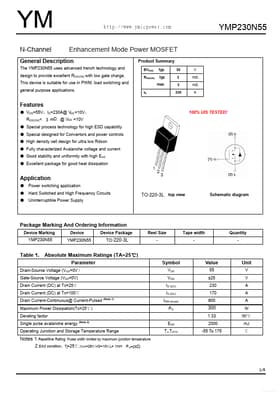
TO-220-3L top view
Schematic diagram
Package Marking And Ordering Information
Device Marking YMP230N55 Device YMP230N55 Device Package TO-220-3L Reel Size Tape width Quantity -
Table 1.
Absolute Maximum Ratings (TA=25℃) Parameter
Symbol
VDS VGS ID (DC) ID (DC)
Value
55 ±25 230 170 900
Unit
V V A A A W W/℃ mJ ℃
Drain-Source
Voltage (VGS=0V) Gate-Source
Voltage (VDS=0V) Drain Current (DC) at Tc=25℃ Drain Current (DC) at Tc=100℃ Drain Current-Continuous@ Current-Pulsed Maximum Power Dissipation(Tc=25℃) Derating factor Single pulse avalanche energy
(Note 2) (Note 1)
IDM (pluse) PD EAS TJ,TSTG
300
1.33 2000 -55 To 175
Operating Junction and Storage Te...