SOT223 N-CHANNEL ENHANCEMENT MODE VERTICAL DMOS FET
ISSUE 3 - JANUARY 1996 7 FEATURES * Compact geometry * Fast switchin...
SOT223 N-CHANNEL ENHANCEMENT MODE VERTICAL DMOS FET
ISSUE 3 - JANUARY 1996 7 FEATURES * Compact geometry * Fast switching speeds * No secondary breakdown and Excellent temperature stability * High input impedance and low current drive * Ease of parralleling
ZVN4206G
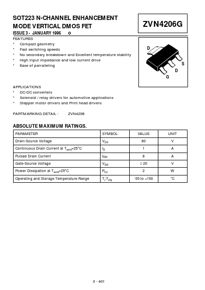
D
S D G
APPLICATIONS * DC-DC converters * Solenoid / relay drivers for automotive applications * Stepper motor drivers and Print head drivers PARTMARKING DETAIL ZVN4206
ABSOLUTE MAXIMUM RATINGS.
PARAMETER Drain-Source
Voltage Continuous Drain Current at Tamb=25°C Pulsed Drain Current Gate-Source
Voltage Power Dissipation at Tamb=25°C Operating and Storage Temperature Range SYMBOL VDS ID IDM VGS Ptot Tj:Tstg VALUE 60 1 8 ± 20 2 -55 to +150 UNIT V A A V W °C
3 - 401
ZVN4206G
ELECTRICAL CHARACTERISTICS (at Tamb = 25°C unless otherwise stated).
PARAMETER SYMBOL MIN. 60 1.3 3 100 10 100 3 1 1.5 300 100 60 20 8 12 12 15 MAX. UNIT CONDITIONS. V V nA µA µA A Ω Ω mS pF pF pF ns ns ns ns VDD ≈25V, ID=1.5A, VGEN =10V VDS=25V, VGS=0V, f=1MHz ID=1mA, VGS=0V ID=1mA, VDS= VGS VGS=± 20V, VDS=0V VDS=60V, VGS=0V VDS=48V, VGS=0V, T=125°C(2) VDS=25V, VGS=10V VGS=10V, ID=1.5A VGS=5V, ID=0.5A VDS=25V,ID=1.5A Drain-Source Breakdown
Voltage BV DSS Gate-Source Threshold
Voltage Gate-Body Leakage Zero Gate
Voltage Drain Current On-State Drain Current (1) Static Drain-Source On-State Resistance (1) VGS(th) IGSS IDSS ID(on) RDS(on)
Forward Transconductance (1)(2) gfs Input Capacitance (2) Common Source Output Capacitance (2) Reverse T...