ZXM62N02E6
20V N-CHANNEL ENHANCEMENT MODE MOSFET
SUMMARY V(BR)DSS=20V; RDS(ON)= 0.1⍀; ID=3.2A
DESCRIPTION This new gene...
ZXM62N02E6
20V N-CHANNEL ENHANCEMENT MODE
MOSFET
SUMMARY V(BR)DSS=20V; RDS(ON)= 0.1⍀; ID=3.2A
DESCRIPTION This new generation of high density
MOSFETs from Zetex utilise a unique structure that combines the benefits of low on-resistance with fast switching speed. This makes them ideal for high efficiency, low
voltage, power management applications. FEATURES
www.DataSheet4U.com
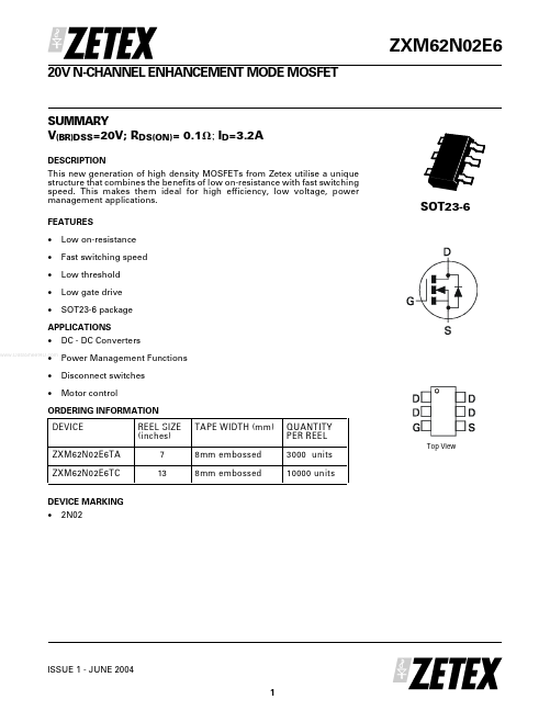
SOT23-6
Low on-resistance Fast switching speed Low threshold Low gate drive SOT23-6 package
APPLICATIONS DC - DC Converters Power Management Functions Disconnect switches Motor control
ORDERING INFORMATION
DEVICE ZXM62N02E6TA ZXM62N02E6TC REEL SIZE (inches) 7 13 TAPE WIDTH (mm) 8mm embossed 8mm embossed QUANTITY PER REEL
Top View
3000 units 10000 units
DEVICE MARKING 2N02
ISSUE 1 - JUNE 2004
1
ZXM62N02E6
ABSOLUTE MAXIMUM RATINGS.
PARAMETER Drain-Source
Voltage Gate Source
Voltage Continuous Drain Current (V GS=4.5V; T A=25°C)(b) (V GS=4.5V; T A=70°C)(b) Pulsed Drain Current (c) Continuous Source Current (Body Diode) (b) Pulsed Source Current (Body Diode) Power Dissipation at T A=25°C (a) Linear Derating Factor Power Dissipation at T A=25°C (b) Linear Derating Factor SYMBOL V DSS V GS ID I DM IS I SM PD PD LIMIT 20 ± 12 3.2 2.6 18 2.1 18 1.1 8.8 1.7 13.6 UNIT V V A A A A W mW/°C W mW/°C
THERMAL RESISTANCE
PARAMETER Junction to Ambient (a) Junction to Ambient (b) SYMBOL R θJA R θJA VALUE 113 73 UNIT °C/W °C/W
NOTES (a) For a device surface mounted on 25mm x 25mm FR4 PCB with...