DATA SHEET
MOS FIELD EFFECT TRANSISTOR
μ PA2755AGR
SWITCHING N-CHANNEL POWER MOS FET
DESCRIPTION The μ PA2755AGR is Dua...
DATA SHEET
MOS FIELD EFFECT TRANSISTOR
μ PA2755AGR
SWITCHING N-CHANNEL POWER MOS FET
DESCRIPTION The μ PA2755AGR is Dual N-channel MOS Field Effect Transistor designed for DC/DC converters and power management applications of notebook computers.
FEATURES Dual chip type Low on-state resistance
RDS(on)1 = 18 mΩ MAX. (VGS = 10 V, ID = 4.0 A) RDS(on)2 = 29 mΩ MAX. (VGS = 4.5 V, ID = 4.0 A) Low input capacitance Ciss = 650 pF TYP. Built-in G-S protection diode Small and surface mount package (Power SOP8)
1.8 MAX.
1.44
0.05 MIN.
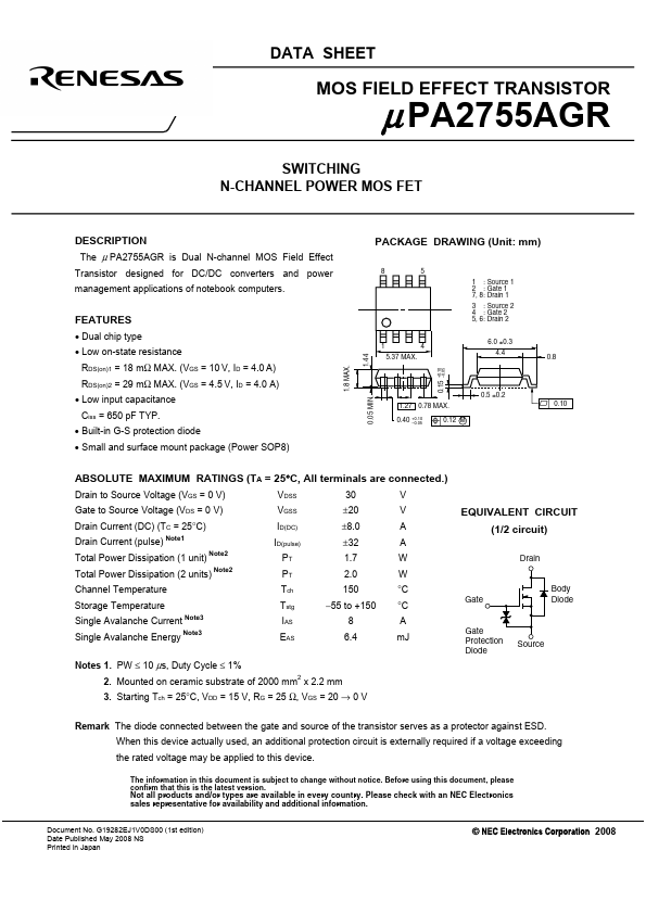
PACKAGE DRAWING (Unit: mm)
85
14 5.37 MAX.
1 : Source 1 2 : Gate 1 7, 8: Drain 1 3 : Source 2 4 : Gate 2 5, 6: Drain 2
6.0 ±0.3 4.4
0.8
+0.10 –0.05
0.15
1.27 0.78 MAX.
0.40
+0.10 –0.05
0.12 M
0.5 ±0.2
0.10
ABSOLUTE MAXIMUM RATINGS (TA = 25°C, All terminals are connected.)
Drain to Source
Voltage (VGS = 0 V)
VDSS
30 V
Gate to Source
Voltage (VDS = 0 V)
VGSS
±20 V
Drain Current (DC) (TC = 25°C) Drain Current (pulse) Note1 Total Power Dissipation (1 unit) Note2 Total Power Dissipation (2 units) Note2
ID(DC) ID(pulse)
PT PT
±8.0 A ±32 A 1.7 W 2.0 W
Channel Temperature
Tch 150 °C
Storage Temperature Single Avalanche Current Note3 Single Avalanche Energy Note3
Tstg −55 to +150 °C IAS 8 A EAS 6.4 mJ
Notes 1. PW ≤ 10 μs, Duty Cycle ≤ 1% 2. Mounted on ceramic substrate of 2000 mm2 x 2.2 mm
3. Starting Tch = 25°C, VDD = 15 V, RG = 25 Ω, VGS = 20 → 0 V
EQUIVALENT CIRCUIT (1/2 circuit)
Drain
Gate
Body Diode
Gate Protection ...