Search by part number and manufacturer or description
 File Size : 60.00KB
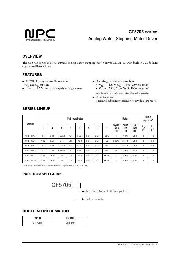
Name VSS VDD XT XTN OUT1 OUT2 RESET TEST Description Negative supply voltage Positive supply voltage Cr ystal oscillator circuit input Cr ystal oscillator circuit output Stepping motor driver output 1 Stepping motor driver output 2 Reset input Test mode select. 512 Hz clock output Pin nu m b e r : .
s
s
32.768 kHz crystal oscillator circuit CG and CD built-in −3.6 to −1.2 V operating supply voltage range
s
Operating current consumption
• VSS =
–1.55V, CD = 16pF: 250 nA (max)
• VSS =
–2.8V, CD = 26pF: 1000 nA (max)
Note: Current consumption depends on the built-in capacitor.
s
Reset function 4 Hz and subsequent frequency dividers are reset
SERIES LINEUP
P ad coordinates Version 1 CF5705AA CF5705BC CF5705AD CF5705AE CF5705CF CF5705CG XT VSS XT XT VSS VSS 2 XTN RESET XTN XTN TEST TEST 3 RESET XT RESET RESET XTN XTN 4 VSS XTN VSS VSS XT XT 5 TEST VDD TEST TEST VDD VDD 6 OUT2 OUT2 OUT2 .


Similar Product
| No. | Part # | Manufacture | Description | Datasheet |
|---|---|---|---|---|
| 1 | CF5705AA |

Nippon Precision Circuits Inc |
Analog Watch Stepping Motor Driver |

|
| 2 | CF5705AD |
Nippon Precision Circuits Inc |
Analog Watch Stepping Motor Driver |
|
| 3 | CF5705AE |
Nippon Precision Circuits Inc |
Analog Watch Stepping Motor Driver |
|
| 4 | CF5705CF |
Nippon Precision Circuits Inc |
Analog Watch Stepping Motor Driver |
|
| 5 | CF5705CG |
Nippon Precision Circuits Inc |
Analog Watch Stepping Motor Driver |
|