Search by part number and manufacturer or description
 File Size : 264.71KB
Pin # Symbol Description 1 D2 Drain of configurable driver #2 2 S2 Source of configurable driver #2 3 S1 Source of configurable driver #1 4 D1 Drain of configurable driver #1 5 CSB SPI Chip Select “Bar” (100 kW pullup resistor to VCC) 6 SCLK SPI clock (100 kW pulldown resistor) 7 SI SP.
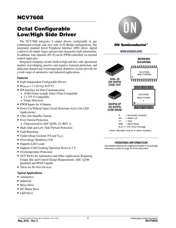
• Eight Independent Configurable Drivers
• RDS(on) = 1.2 W (typ @25°C)
• SPI Interface for Data Communication
♦ 16 Bit Frame Length, Daisy Chain Compatible ♦ 3.3 V/5 V Compatible ♦ Frame Detection
• PWM Inputs for 4 Outputs
• Ultra−low Standby Current
• Over Current Protection
♦ Characterized to AEC Q10X−12−REV A
• High−Side and Low−Side Flyback Protection
• Fault Repoting
• Undervoltage Lockout (VS and VCC)
• Overvoltage Shutdown (VS)
• Supports LED Loads
• Supports Cold Cranking Operation Down to 3 V
• Overtemperature Protection
• NCV Prefix for Automotive and Other Applications Requiring
Un.


Similar Product
| No. | Part # | Manufacture | Description | Datasheet |
|---|---|---|---|---|
| 1 | NCV760040 |

ON Semiconductor |
Quad High-side Driver |

|
| 2 | NCV7601 |
ON Semiconductor |
Quad Driver |
|
| 3 | NCV7680 |
ON Semiconductor |
Linear Current Regulator/Controller |
|
| 4 | NCV7681 |
ON Semiconductor |
100mA Linear Current Regulator/Controller |
|
| 5 | NCV7683 |
ON Semiconductor |
Enhanced 100mA Linear Current Regulator/Controller |
|