Search by part number and manufacturer or description
 File Size : 413.68KB
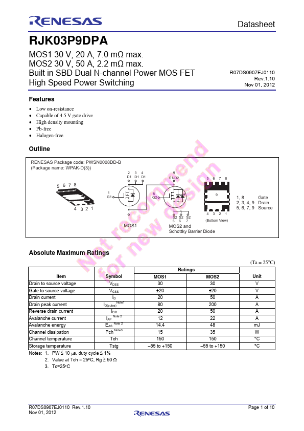
Preliminary Datasheet RJK03P9DPA MOS1 30 V, 20 A, 7.0 mΩ max. MOS2 30 V, 50 A, 2.2 mΩ max. Built in SBD Dual N-channel Power MOS FET High Speed Power Switching R07DS0907EJ0110 Rev.1.10 Nov 01, 2012 Features Low on-resistance Capable of 4.5 V gate drive High density mounting Pb-free Halo.
Low on-resistance
Capable of 4.5 V gate drive
High density mounting
Pb-free
Halogen-free
Outline
RENESAS Package code: PWSN0008DD-B (Package name: WPAK-D(3))
5 678
1 G1
234 D1 D1 D1
8 G2
4 32 1
MOS1
9 S1/D2
5678
9
S2 S2 S2 56 7
4321 (Bottom View)
MOS2 and
Schottky Barrier Diode
1, 8 Gate 2, 3, 4, 9 Drain 5, 6, 7, 9 Source
Absolute Maximum Ratings
Item
Symbol
Drain to source voltage Gate to source voltage Drain current Drain peak current Reverse drain current Avalanche current Avalanche energy Channel dissipation
VDSS
VGSS
ID ID(pulse)Note1
IDR IAP Note 2 EAS Note .


Similar Product
| No. | Part # | Manufacture | Description | Datasheet |
|---|---|---|---|---|
| 1 | RJK03P7DPA |

Renesas Technology |
Dual N-Channel Power MOSFET |

|
| 2 | RJK0301DPB |
Renesas Technology |
Silicon N Channel Power MOS FET Power Switching |
|
| 3 | RJK0302DPB |
Renesas Technology |
Silicon N Channel Power MOS FET Power Switching |
|
| 4 | RJK0303DPB |
Renesas Technology |
Silicon N Channel Power MOS FET Power Switching |
|
| 5 | RJK0304DPB |
Renesas Technology |
Silicon N Channel Power MOS FET Power Switching |
|