| Part Number | A35S |
| Manufacturer | Thinki Semiconductor |
| Title | 35.0 Ampere Avalanche Rectifier Diodes |
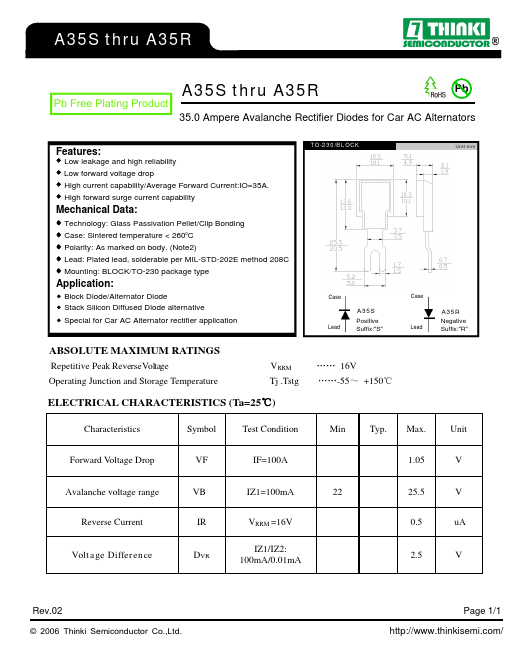
| Description | A35S thru A35R ® A35S thru A35R Pb Pb Free Plating Product 35.0 Ampere Avalanche Rectifier Diodes for Car AC Alternators Features: Low leaka... |
| Features |
Low leakage and high reliability Low forward voltage drop High current capability/Average Forward Current:IO=35A. High forward surge current capability
Mechanical Data:
Technology: Glass Passivation Pellet/Clip Bonding Case: Sintered temperature 260oC Polarity: As marked on body. (Note2) Lead: Pl...
|
| File Size | 332.77KB |
| Datasheet |
|


A3-44PA-2SV : Pin Name A0 ~ A12 BA0 ~ BA1 DQ0 ~ DQ63 DQS0 ~ DQS17 CK0,CK0 ~ CK2, CK2 CKE0, CKE1(for double banks) CS0, CS1(for double banks) RAS CAS WE CB0 ~ CB7 Function Address input (Multiplexed) Bank Select Address Data input/output Data Strobe input/output Clock input Clock enable input Chip select input Row address strobe Column address strobe Write enable Check bit(Data-in/data-out) Pin Name DM0 ~ DM8 VDD VDDQ VSS VREF VDDSPD SDA SCL SA0 ~ 2 NC Data - in mask Power supply (2.5V for DDR266/333, 2.6V for DDR400) Power Supply for DQS (2.5V for DDR266/333, 2.6V for DDR400) Ground Power supply for reference Serial EEPROM Power/Supply ( 2.3V to 3.6V ) Serial data I/O Serial clock Address in EEPROM No con.
A3-xxxA-2xx : Pin Name A0 ~ A12 BA0 ~ BA1 DQ0 ~ DQ63 DQS0 ~ DQS17 CK0,CK0 ~ CK2, CK2 CKE0, CKE1(for double banks) CS0, CS1(for double banks) RAS CAS WE CB0 ~ CB7 Function Address input (Multiplexed) Bank Select Address Data input/output Data Strobe input/output Clock input Clock enable input Chip select input Row address strobe Column address strobe Write enable Check bit(Data-in/data-out) Pin Name DM0 ~ DM8 VDD VDDQ VSS VREF VDDSPD SDA SCL SA0 ~ 2 NC Data - in mask Power supply (2.5V for DDR266/333, 2.6V for DDR400) Power Supply for DQS (2.5V for DDR266/333, 2.6V for DDR400) Ground Power supply for reference Serial EEPROM Power/Supply ( 2.3V to 3.6V ) Serial data I/O Serial clock Address in EEPROM No con.
A3010 : . -=4 5 0 . 6 / ; 7?6@4 5- 2AB?4 2A;9* 0 -=4 5 @= 5A++ (4 -( ;24 A2 7? 6? @A A@ 9 0 4 56? 7? 6? '= ( C . 6 / ) / 0 $ " = " # =! 2 =3 ! , ! " !3 2 # "& D , !E " " $ "! !$ $ !,# $ # ! ! " ," D & !, , - = A D F # ,! # & 3 # ! " 3 D D! %$ ! & !, " F $ ; # $## & $# !, , % $ ! !, $ !D $ ! $ " 3 3 , . * / $! ! ! $! $ !, # ! 2 ! " ## ! $ !# , 7* # F , " & E ! '4 @*+ ;* ! ! ! !, 3 D 1 ) 0/ 2 = = G G ) 3 ! ! 2 ( 30 7* +'= !! # ! ) www.DataSheet4U.com G G " !! ! " # ! &' % %$ ! & + + ,! - ! 2 3 5 6 8 0 ! 4 ,$ . - ! . !/ . ! / / '() 0 0 0 0 0 0 / 9 / = 9 9 9 1 1 1 $ 2 + ; , 4 5 # # , $ $ 6 2 4 5 * H 0 9 H 9 9 0 : H ( * * ) " +* * !* * * , * -- ! !$ $ 4 !#$ 6 +" ..
A301D : www.DataSheet.in www.DataSheet.in www.DataSheet.in .
A301V : www.DataSheet.in www.DataSheet.in www.DataSheet.in .
A3046 : 3046, 3056, AND 3058 The A3046EU/LU, A3056EU/LU, and A3058EU/LU Hall effect gear-tooth sensors are monolithic integrated circuits that switch in response to differential magnetic fields created by ferrous targets. These devices are ideal for use in gear-tooth-based speed, position, and timing applications and operate down to zero rpm over a wide range of air gaps and temperatures. When combined with a backbiasing magnet and proper assembly techniques, devices can be configured to give 50% duty cycle or to switch on either leading, trailing, or both edges of a passing gear tooth or slot. HALL EFFECT GEAR-TOOTH SENSORS –ZERO SPEED Data Sheet 27612A† X X V CC 1 2 3 GROUND OUTPUT SUP.
A3054 : Data Sheet 27680.1 3054 MULTIPLEXED TWO-WIRE 3054 HALL-EFFECT SENSOR ICs LOGIC 12 3 BUS GROUND SWITCH IN Dwg. PH-005 Pinning is shown viewed from branded side. ABSOLUTE MAXIMUM RATINGS at TA = +25°C Supply Voltage, VBUS . . 18 V Magnetic Flux Density, B . Unlimited Operating Temperature Range, TA A3054KU . . -40°C to +125°C A3054SU -20°C to +85°C Storage Temperature Range, TS . . -55°C to +150°C Package Power Dissipation, PD . . 635 mW X MULTIPLEXED TWO-WIRE HALL-EFFECT SENSOR ICs The A3054KU and A3054SU Hall-effect sensors are digita.
A3056 : Data Sheet 27612A† 3046, 3056, AND 3058 HALL EFFECT GEAR-TOOTH SENSORS –ZERO SPEED XX V CC 12 3 SUPPLY GROUND OUTPUT Dwg. PH-012 Pinning is shown viewed from branded side. ABSOLUTE MAXIMUM RATINGS Supply Voltage, VCC . . 28 V Reverse Battery Voltage, VRCC . -30 V Magnetic Flux Density, B . . Unlimited Output OFF Voltage, VOUT 28 V Reverse Output Voltage, VOUT . . -0.5 V Output Current, IOUT 25 mA Package Power Dissipation, PD . . 500 mW Operating Temperature Range, TA Suffix “EU” -40°C to +85°C Suffix “LU” . . -40°C to +150°C Storage Te.
A3058 : Data Sheet 27612A† 3046, 3056, AND 3058 HALL EFFECT GEAR-TOOTH SENSORS –ZERO SPEED XX V CC 12 3 SUPPLY GROUND OUTPUT Dwg. PH-012 Pinning is shown viewed from branded side. ABSOLUTE MAXIMUM RATINGS Supply Voltage, VCC . . 28 V Reverse Battery Voltage, VRCC . -30 V Magnetic Flux Density, B . . Unlimited Output OFF Voltage, VOUT 28 V Reverse Output Voltage, VOUT . . -0.5 V Output Current, IOUT 25 mA Package Power Dissipation, PD . . 500 mW Operating Temperature Range, TA Suffix “EU” -40°C to +85°C Suffix “LU” . . -40°C to +150°C Storage Te.
A306 : .
A3064 : Data Sheet 27612.21 3064 HALL-EFFECT GEAR-TOOTH SENSOR —AC COUPLED SUPPLY OUTPUT GROUND FILTER FILTER XX VCC 12 34 5 Dwg. PH-011-1 Pinning is shown viewed from branded side. ABSOLUTE MAXIMUM RATINGS at TA = +25°C Supply Voltage, VCC ..... 24 V Reverse Battery Voltage, VRCC .... -30 V Magnetic Flux Density, B Unlimited Output Off Voltage, VOUT .... 24 V Output Current, IOUT . 25 mA Package Power Dissipation, PD .. 500 mW Operating Temperature Range, TA . -40°C to +150°C Storage Temperature Range, TS . -65.
A3064 : G.6.C! R.F. PENTODE A3064 - VALVES ISSUE 1 An r. f. pentode suitable for use in applications where long life and close control of characteristics are required. - The A3064 will replace the CV138, CV4014 and Z77 in most applications. BASE CONNECTIONS AND VALVE DIMENSIONS Ih ha Base: Small-button miniature (B7G) Bulb: Tubular k g3,S Max. overall length : 54.5mm Max. seated length: 47.5mm gl gz Max. diameter: 19mm Viewed from underside of base. 6.3 V 0.3 A MAXIMUM RATINGS (Absolute) Va(o) Va 550 300 Pa I Vg2(o) Vg2 Pg2 2.5 450 300 0.8 Rgl-k 0.5 Vh-k (heater positive) 100 -Vh-k (heater negative) 250 Tbulb 200 V V W V V W MQ V V °C CAPACITANCES (Measured on a.
A3064 : G.6.C! R.F. PENTODE A3064 - VALVES ISSUE 1 An r. f. pentode suitable for use in applications where long life and close control of characteristics are required. - The A3064 will replace the CV138, CV4014 and Z77 in most applications. BASE CONNECTIONS AND VALVE DIMENSIONS Ih ha Base: Small-button miniature (B7G) Bulb: Tubular k g3,S Max. overall length : 54.5mm Max. seated length: 47.5mm gl gz Max. diameter: 19mm Viewed from underside of base. 6.3 V 0.3 A MAXIMUM RATINGS (Absolute) Va(o) Va 550 300 Pa I Vg2(o) Vg2 Pg2 2.5 450 300 0.8 Rgl-k 0.5 Vh-k (heater positive) 100 -Vh-k (heater negative) 250 Tbulb 200 V V W V V W MQ V V °C CAPACITANCES (Measured on a.
A31 : Initial version Modify the A31 block diagram Revise video output spec Revise the logo Modify the electrical characteristic section Modify Pin Description A31 Datasheet (Revision 1.4) Copyright © 2013 Allwinner Technology. All Rights Reserved. Page 1 A31 Datasheet DECLARATION THIS A31 DATASHEET IS THE ORIGINAL WORK AND COPYRIGHTED PROPERTY OF ALLWINNER TECHNOLOGY (“ALLWINNER”). REPRODUCTION IN WHOLE OR IN PART MUST OBTAIN THE WRITTEN APPROVAL OF ALLWINNER AND GIVE CLEAR ACKNOWLEDGEMENT TO THE COPYRIGHT OWNER. THE INFORMATION FURNISHED BY ALLWINNER IS BELIEVED TO BE ACCURATE AND RELIABLE. ALLWINNER RESERVES THE RIGHT TO MAKE CHANGES IN CIRCUIT DESIGN AND/OR SPECIFICATIONS AT ANY TIME WITHO.
A31-1 : A31-1/SMA31-1 10 TO 2000 MHz CECASCADABLE AMPLIFIER · LOW NOISE: 3.5 dB (TYP.) · LOW VSWR: 1.5:1 (TYP.) Typical Performance @ 25°C Specifications (Rev. Date: 1/01)* Characteristics Frequency Small Signal Gain (min.) Gain Flatness (max.) Reverse Isolation Noise Figure (max.) Power Output @ 1 dB comp. (min.) IP3 IP2 Second Order Harmonic IP VSWR Input / Output (max.) DC Current @ 15 Volts (max.) Typical 0° to 50°C Guaranteed -54° to +85°C 0.0-2.1 GHz 11.5 dB ±0.4 dB 17 dB 3.5 dB -2.0 dBm +9 dBm +10 dBm +15 dBm 1.5:1 / 1.3:1 9 mA 0.0-2.0 GHz 11.0 dB ±0.7 dB 4.0 dB -4.0 dBm 0.0-2.0 GHz 10.5 dB ±1.0 dB 4.5 dB -4.5 dBm 2.0:1 / 2.0:1 11 mA 2.0:1 / 2.0:1 12 mA * Measured in a 50-ohm syste.
A310 : .
A31101AP : www.DataSheet4U.com www.DataSheet4U.com www.DataSheet4U.com www.DataSheet4U.com www.DataSheet4U.com www.DataSheet4U.com www.DataSheet4U.com www.DataSheet4U.com www.DataSheet4U.com www.DataSheet4U.com www.DataSheet4U.com www.DataSheet4U.com .