v2.0
General-Purpose SDRAM Controller
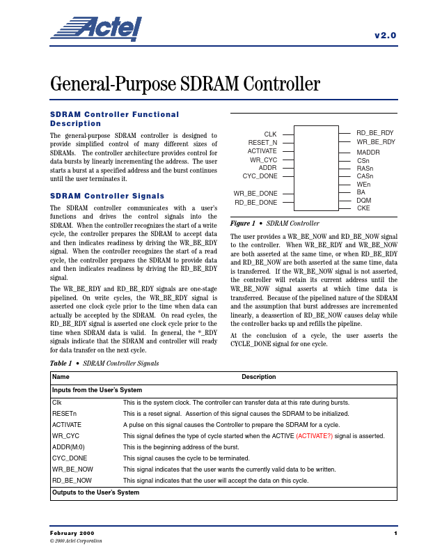
SD R A M Co n t r o l l er Fu nc t i o na l D es cr i p t i o n
The general-purpose SDRAM controller is designed to provide simplified control of many different sizes of SDRAMs. The controller architecture provides control for data bursts by linearly incrementing the address. The user starts a burst at a specified addr...