| Part Number | 5PB1108PGG |
| Manufacturer | IDT |
| Description | 1.8V to 3.3V LVCMOS High-Performance Clock Buffer |
| Published | Jan 27, 2019 |
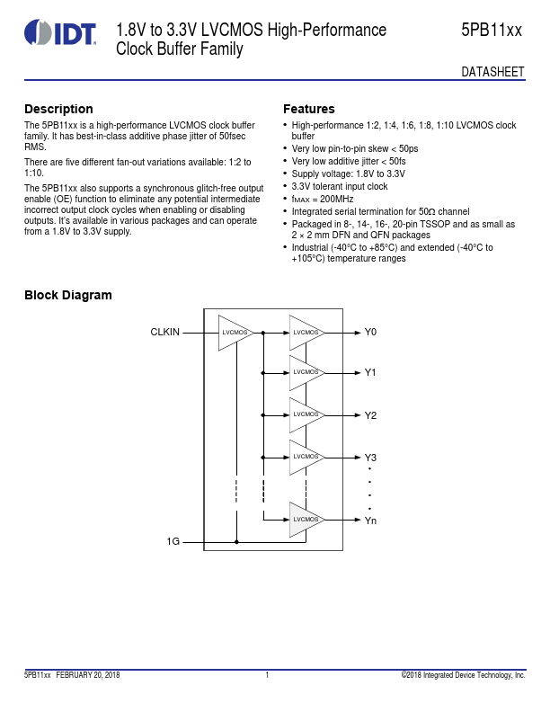
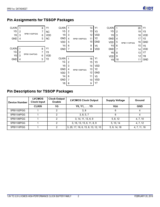
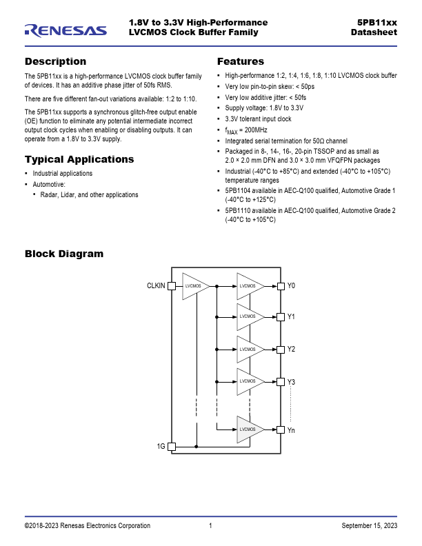
| Detailed Description | 1.8V to 3.3V LVCMOS High-Performance Clock Buffer Family 5PB11xx DATASHEET Description The 5PB11xx is a high-performan... |
| Datasheet |
|