| Part Number | 5PB1213 |
| Manufacturer | Renesas |
| Description | TCXO/LVCMOS Clock Buffer |
| Published | May 19, 2020 |
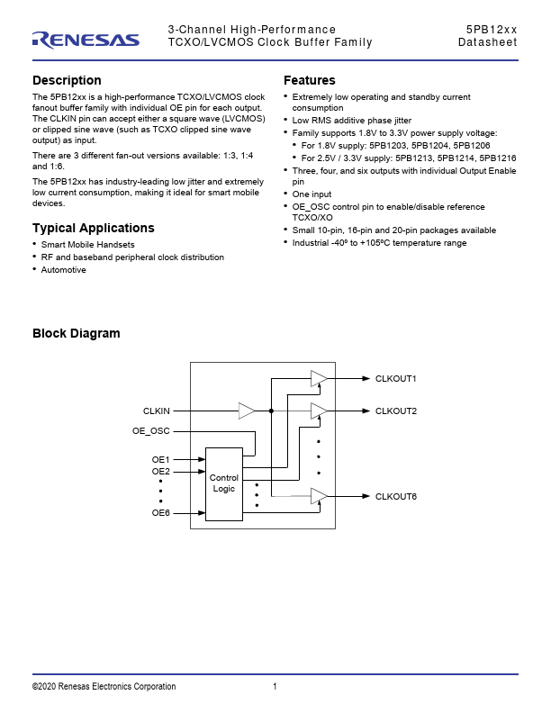
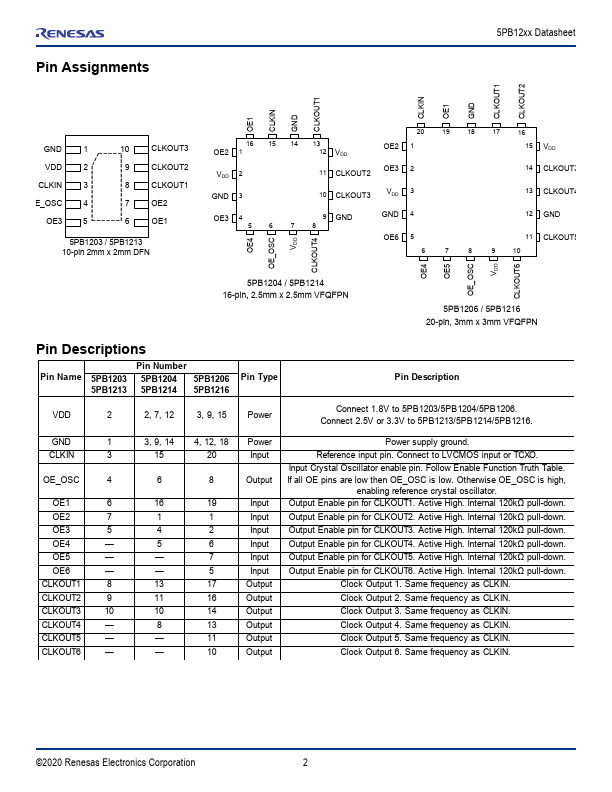
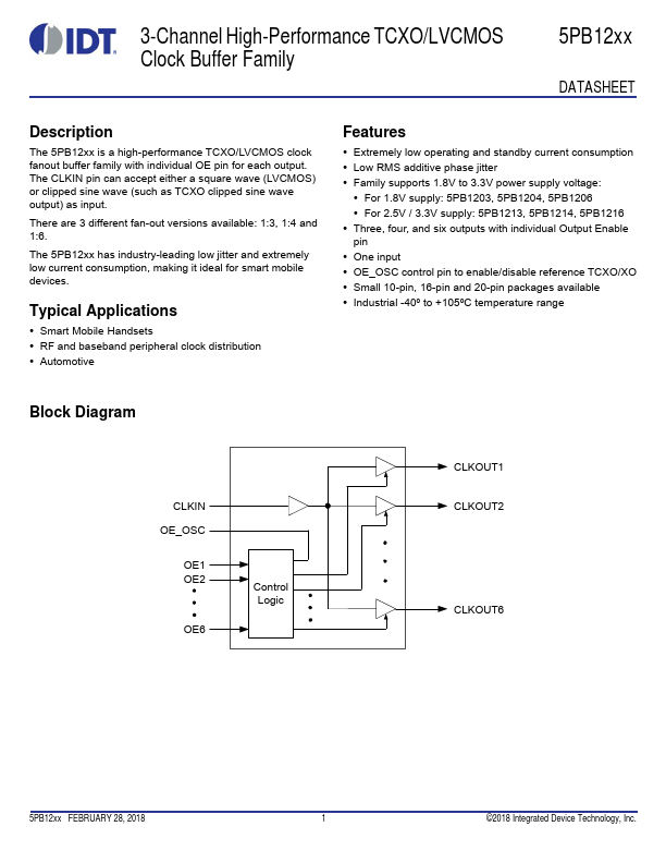
| Detailed Description | 3-Channel High-Performance TCXO/LVCMOS Clock Buffer Family 5PB12xx Datasheet Description The 5PB12xx is a high-perform... |
| Datasheet |
|