| Part Number | 9DB233 |
| Manufacturer | IDT |
| Description | Two Output Differential Buffer |
| Published | Dec 13, 2016 |
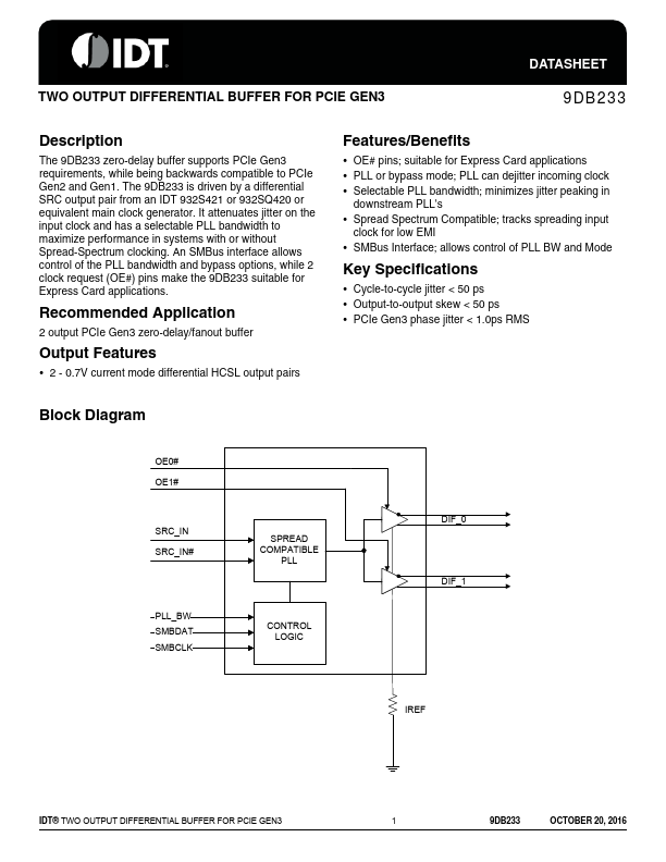
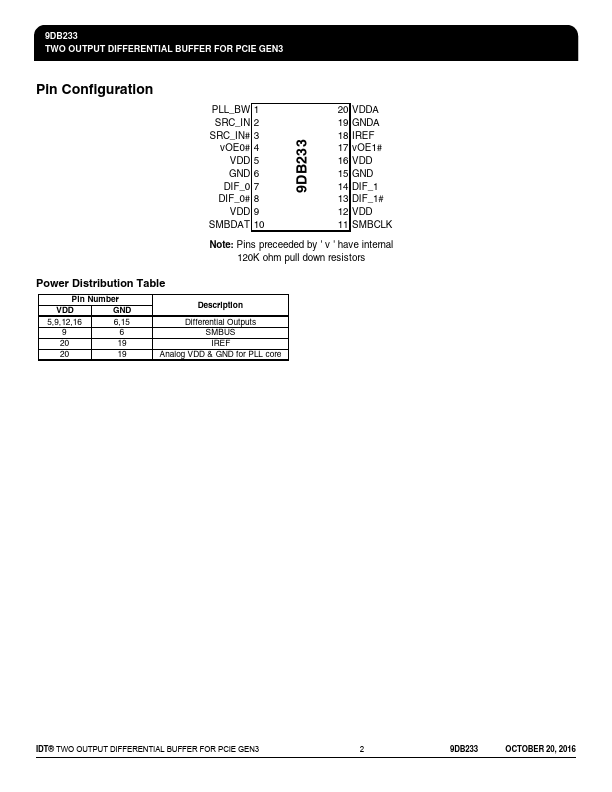
| Detailed Description | DATASHEET Two Output Differential Buffer for PCIe Gen3 9DB233 Recommended Application: 2 output PCIe Gen3 zero-delay/... |
| Datasheet |
|