VDS 1000 V
C3M0120100J
ID @ 25˚C
22 A
Silicon Carbide Power MOSFET TM
C3M MOSFET Technology
RDS(on) 120 mΩ
N-Channel Enhancement Mode
Features
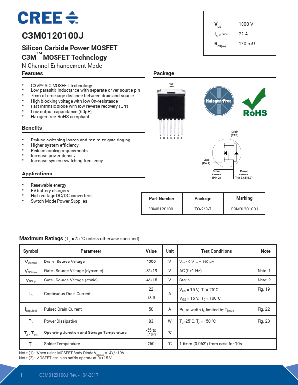
Package
C3MTM SiC MOSFET technology Low parasitic inductance with separate driver source pin 7mm of creepage distance between drain and source High blocking voltage with low On...