![]() |
Amplifier. LMC6024 Datasheet |
|
![]() November 1994
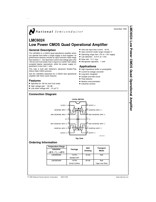
LMC6024
Low Power CMOS Quad Operational Amplifier
General Description
The LMC6024 is a CMOS quad operational amplifier which
can operate from either a single supply or dual supplies. Its
performance features include an input common-mode range
that reaches V−, low input bias current and voltage gain (into
100 kΩ and 5 kΩ loads) that is equal to or better than widely
accepted bipolar equivalents, while the power supply re-
quirement is less than 1 mW.
This chip is built with National’s advanced Double-Poly
Silicon-Gate CMOS process.
See the LMC6022 datasheet for a CMOS dual operational
amplifier with these same features.
Features
n Specified for 100 kΩ and 5 kΩ loads
n High voltage gain 120 dB
n Low offset voltage drift 2.5 µV/˚C
n Ultra low input bias current 40 fA
n Input common-mode range includes V−
n Operating range from +5V to +15V supply
n Low distortion 0.01% at 1 kHz
n Slew rate 0.11 V/µs
n Micropower operation 1 mW
Applications
n High-impedance buffer or preamplifier
n Current-to-voltage converter
n Long-term integrator
n Sample-and-hold circuit
n Peak detector
n Medical instrumentation
n Industrial controls
Connection Diagram
14-Pin DIP/SO
Ordering Information
Temperature Range
Industrial
−40˚C ≤ TJ ≤ +85˚C
LMC6024IN
LMC6024IM
Top View
Package
14-Pin
Molded DIP
14-Pin
Small Outline
NSC
Drawing
N14A
M14A
DS011235-1
Transport
Media
Rail
Rail
Tape and Reel
© 1999 National Semiconductor Corporation DS011235
www.national.com
|
|
![]() Absolute Maximum Ratings (Note 1)
If Military/Aerospace specified devices are required,
please contact the National Semiconductor Sales Office/
Distributors for availability and specifications.
Differential Input Voltage
Supply Voltage (V+ − V−)
Lead Temperature
(Soldering, 10 sec.)
Storage Temperature Range
Voltage at Output/Input Pin
Current at Input Pin
Current at Output Pin
Current at Power Supply Pin
Output Short Circuit to V+
±Supply Voltage
16V
260˚C
−65˚C to +150˚C
(V+) + 0.3V, (V−) − 0.3V
±5 mA
±18 mA
35 mA
(Note 12)
Output Short Circuit to V−
Junction Temperature
ESD Tolerance (Note 4)
Power Dissipation
Operating Ratings
Temperature Range
Supply Voltage Range
Power Dissipation
Thermal Resistance (θJA), (Note 11)
14-Pin DIP
14-Pin SO
(Note 2)
150˚C
1000V
(Note 3)
−40˚C ≤ TJ ≤ +85˚C
4.75V to 15.5V
(Note 10)
85˚C/W
115˚C/W
DC Electrical Characteristics
The following specifications apply for V+ = 5V,
face limits apply at the temperature extremes;
V− = 0V, VCM
all other limits
=
TJ
1=.52V5,˚CVO.
=
2.5V,
and
RL
=
1M
unless
otherwise
noted.
Bold-
Typical
LMC6024I
Symbol
Parameter
Conditions
(Note 5)
Limit
Units
(Note 6)
VOS Input Offset Voltage
1 9 mV
11 Max
∆VOS/∆T
Input Offset Voltage
Average Drift
2.5 µV/˚C
IB Input Bias Current
0.04
pA
200 Max
IOS
RIN
CMRR
Input Offset Current
Input Resistance
Common Mode
Rejection Ratio
0V ≤ VCM ≤ 12V
V+ = 15V
0.01
pA
100 Max
>1 TeraΩ
83 63 dB
61 Min
+PSRR
Positive Power Supply
5V ≤ V+ ≤ 15V
83 63 dB
Rejection Ratio
61 Min
−PSRR
Negative Power Supply
0V ≤ V− ≤ −10V
94 74 dB
Rejection Ratio
73 Min
VCM
Input Common-Mode
Voltage Range
V+ = 5V and 15V
For CMRR ≥ 50 DB
−0.4
−0.1
0
V
Max
V+ − 1.9
V+ − 2.3
V
V+ − 2.5
Min
AV
Large Signal Voltage Gain
RL = 100 kΩ (Note 7)
1000
200 V/mV
Sourcing
100 Min
Sinking
500 90 V/mV
40 Min
RL = 5 kΩ (Note 7)
Sourcing
1000
100 V/mV
75 Min
Sinking
250 50 V/mV
20 Min
www.national.com
2
|
![]() DC Electrical Characteristics (Continued)
The following specifications apply for V+ = 5V,
face limits apply at the temperature extremes;
V− = 0V, VCM
all other limits
=
TJ
1=.52V5,˚CVO.
=
2.5V,
and
RL
=
1M
unless
otherwise
noted.
Bold-
Typical
LMC6024I
Symbol
Parameter
Conditions
(Note 5)
Limit
Units
(Note 6)
VO Output Voltage Swing
V+ = 5V
RL = 100 kΩ to 2.5V
4.987
0.004
4.40
4.43
0.06
V
Min
V
0.09
Max
V+ = 5V
4.940 4.20 V
RL = 5 kΩ to 2.5V
0.040
4.00
0.25
Min
V
0.35
Max
V+ = 15V
14.970
14.00
V
RL = 100 kΩ to 7.5V
0.007
13.90
0.06
Min
V
0.09
Max
V+ = 15V
14.840
13.70
V
RL = 5 kΩ to 7.5V
0.110
13.50
0.32
Min
V
0.40
Max
IO Output Current
V+ = 5V
Sourcing, VO = 0V
Sinking VO = 5V
(Note 2)
22 13 mA
9 Min
21 13 mA
9 Min
V+ = 15V
40 23 mA
Sourcing, VO = 0V
Sinking, VO = 13V
(Note 12)
15 Min
39 23 mA
15 Min
IS Supply Current
All Four Amplifiers
VO = 1.5V
160 240 µA
280 Max
3 www.national.com
|
@ 2014 :: Datasheetspdf.com :: Semiconductors datasheet search & download site (Privacy Policy & Contact) |