1:3 Clock Buffer
Description
SLG3SY3952
1:3 Clock Buffer
OE_26M_A 26M_A 26M_B OE_26M_B 26M_C
General Description
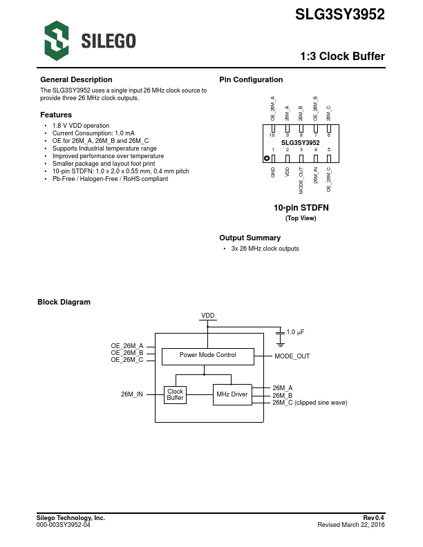
The SLG3SY3952 uses a single input 26 MHz clock source to provide three 26 MHz clock outputs.
Pin Configuration
Features
1.8 V VDD operation Current Consumption: 1.0 mA OE for 26M_A, 26M_B and 26M_C Supports Industrial temperature range Improved performance ove...
Similar Datasheet