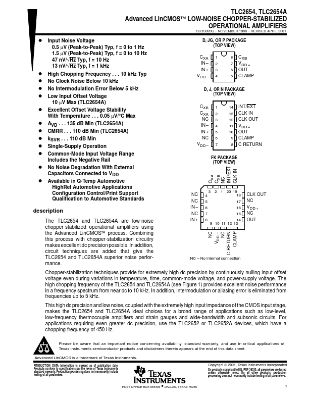
TLC2654, TLC2654A Advanced LinCMOS LOW-NOISE CHOPPER-STABILIZED
OPERATIONAL AMPLIFIERS
SLOS020G – NOVEMBER 1988 – REVISED APRIL 2001
D Input Noise Voltage
0.5 µV (Peak-to-Peak) Typ, f = 0 to 1 Hz 1.5 µV (Peak-to-Peak) Typ, f = 0 to 10 Hz 47 nV/√Hz Typ, f = 10 Hz 13 nV/√Hz Typ, f = 1 kHz
D High Chopping Frequency . . . 10 kHz Typ D No Clock Noise Below 10 k...