DatasheetsPDF.com
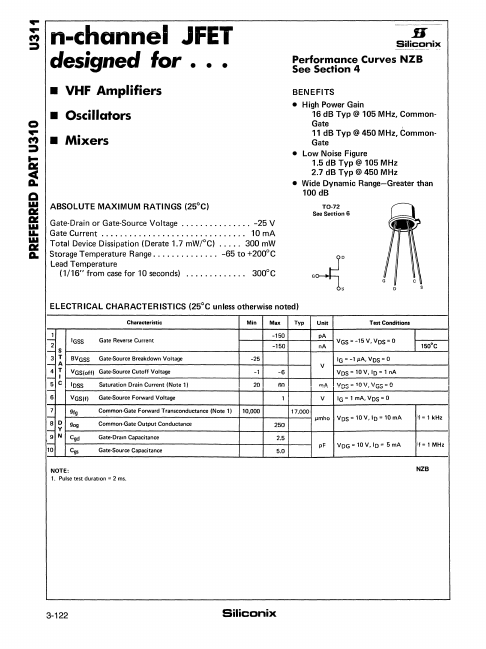
U311
Part Number
U311
Manufacturer
Siliconix
Description
n-channel
JFET
Published
Sep 21, 2019
Datasheet
U311
PDF File
Features
n-channel JFET designed for
•
•
•
• VHF
Amplifier
s
• Oscillators
• Mixers ABSOLUTE MAXIMUM RATINGS (25°C) Gate-Drain or Gate-Source
Voltage
-25 V Gate Current .10mA Total Device Dissipation (Derate 1...
Similar Datasheet
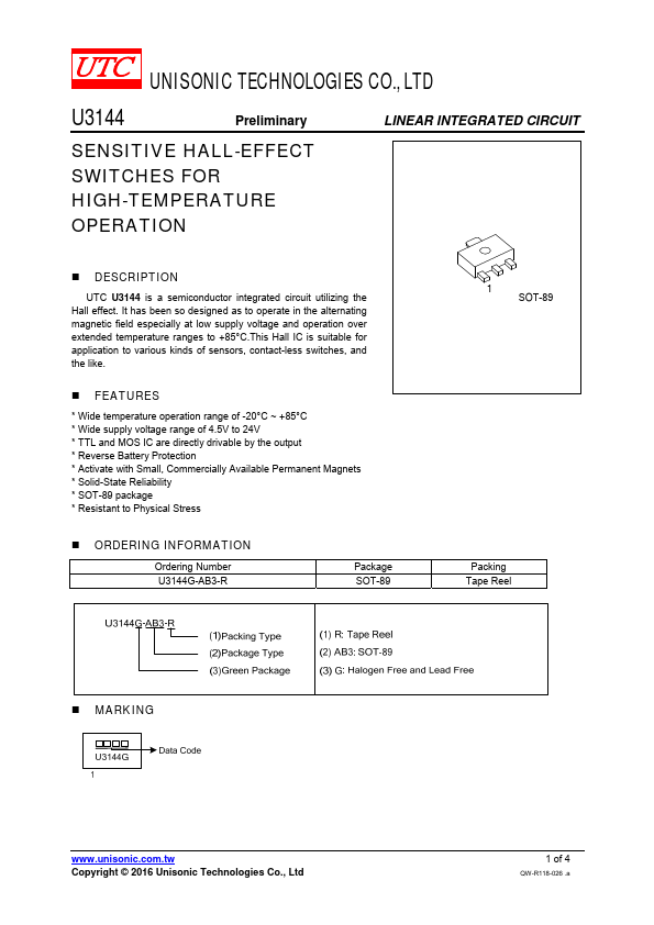
U3144
SENSITIVE HALL-EFFECT SWITCHES
(UTC)
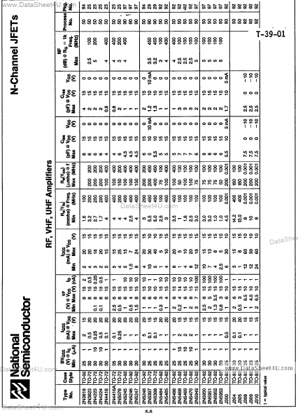
U312
TRANSISTOR
(National Semiconductor)
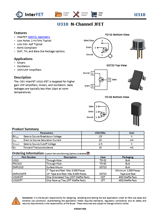
U310
N-Channel JFET
(InterFET)
U310
N-Channel JFETs
(Vishay)
Since 2006. D4U Semicon,
Electronic Components Datasheet Search Site. (
Privacy Policy & Contact
)